
Some Interesting Facts about Rectangular Waveguides
David W. Porterfield, Ph.D., Micro Harmonics Corporation
Rectangular waveguides are commonly used in mm-wave applications primarily because they are the lowest loss transmission media at these frequencies. They are single-moded over broad bandwidths and provide isolation from external RF signals. In this post, we will review some other interesting facts about rectangular waveguides and hopefully provide some helpful tips.
Bandwidth
Standard rectangular waveguide bands have a 40% fractional bandwidth. For example, the standard WR-12 waveguide is defined to cover the band from 60 GHz to 90 GHz. The center frequency is 75 GHz. The fractional bandwidth is (90 GHz – 60 GHz)/(75 GHz) = 40%.
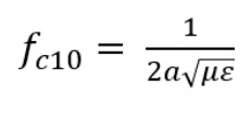
The standard bands are defined in a way that ensures that only a single propagating mode (TE10) exists within the waveguide. This is important so that RF signals can effectively be coupled to and from the waveguides. The equation below gives the cutoff frequency for the TE10 mode in a rectangular waveguide. In this equation, “a” is the broad wall length in meters and “f” is the frequency in Hertz. No RF signals can propagate in the waveguide below the TE10 cutoff frequency.
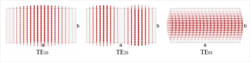
A safety margin is built into the low end of the standard waveguide band to avoid high impedances near the TE10 mode cut-off frequency (more on that in the next section). A safety margin is also provided at the high end of the band to ensure that the next higher order TE20 and TE01 modes cannot propagate in the waveguide. The TE20 and TE01 cutoff frequencies are exactly twice the TE10 cutoff frequency when the waveguide height “b” is half the waveguide width “a”. The sketches below show the electric field distribution in rectangular waveguides for the primary TE10, and the higher order TE20, and TE01 modes.
Impedance
It is a common misconception that rectangular waveguides have a 50 Ω characteristic impedance. Our conception of impedance is often in terms of the ratio of voltage and current. But in rectangular waveguides, the voltages and currents are distributed and non-uniform along the cross-section of the waveguide. One must define where and how the voltages and currents are measured. Here are four common impedance definitions used for rectangular waveguides:
- ZTE and ZTM – These definitions are based on ratios of the transverse electric and magnetic fields.
- Zpi – This impedance is defined in terms of the z-directed power and the integration of the current vector around the periphery of the rectangular waveguide.
- Zpv – Similar to Zpi but in terms of power and voltage. An integration line must be given.
- Zvi – Similar to Zpi and Zpv, but in terms of voltage and current. Zvi = √(Zpi*Zpv).
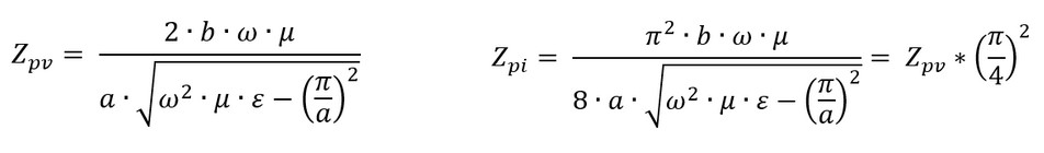
Simple closed-form solutions for Zpv and Zpi are available for the primary TE10 mode as shown below. The equation for Zpv is only valid for the maximum TE10 voltage which is obtained by integrating the electric field along a line at the center of the waveguide (a/2) from -b/2 to +b/2. If a = 2*b (the height is half the width), and using the same integration line, then Zpv = ZTE for the TE10 mode.
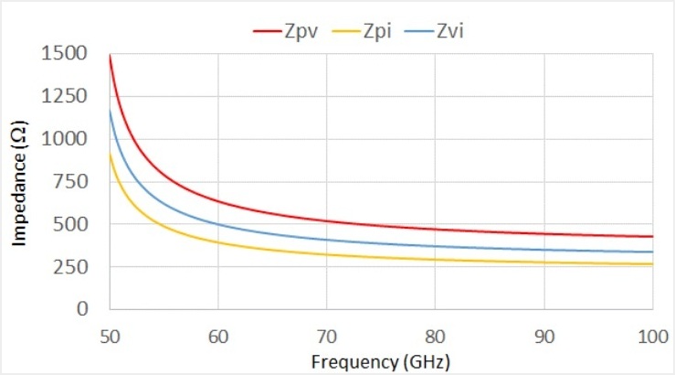
The graph below shows the TE10 mode waveguide impedances Zpv, Zpi, and Zvi. Impedance is relatively flat across the standard WR-12 waveguide band 60-90 GHz which facilitates broadband impedance matching. The impedance increases rapidly at the low end of the band approaching infinity at the TE10 cutoff frequency. We only show the plot down to 50 GHz (the TE10 cutoff is 48.4 GHz in WR-12). Although it is more difficult to obtain broadband matching below the recommended band, it is not impossible. For example, a Micro Harmonics WR-12 Faraday rotation isolator gives good performance over the extended band from 55-95 GHz.
Waveguide Band Designations
The most common waveguide band designations in the US are the EIA. For example, the EIA designation for E-band (60-90 GHz) is WR-12. You probably already knew this. But did you know that the EIA designation is based on one tenth of the waveguide broad wall dimension in mils (1 mil = 0.001 inch)? Unfortunately, there are often roundoffs in the EIA designation. For example, the WR-12 broad wall dimension is 122 mils rather than 120 mils.
The lack of precision in the EIA designation is more problematic at the higher mm-wave frequencies. For example, the WR-6 rectangular waveguide has a 65 mil broad wall rather than 60 mils. To make matters worse, the EIA rounded down to WR-6 rather than up to WR-7, a mathematical heresy! Nowadays you often see folks adding a decimal place in the EIA designation, referring to the WR-6.5 band rather than the WR-6 band, or the WR-3.4 band rather than the WR-3 band. The IEEE has adopted a new standard for waveguides at WR-10 and higher. The IEEE standard specifies the waveguide broad wall in microns. The old WR-10 EIA band became the WM-2540. A waveguide band designed for the 1.1-1.7 THz range is designated as WM-164 rather than WR-0.65. The new standard is a big improvement since it clarifies ambiguities, is metric, and provides tighter tolerancing needed at the higher mm-wave frequencies.
Some Simple Calculations
Approximate calculations of the TE10, TE20, and TE01 cutoff frequencies and the recommended operating frequencies for a waveguide band can quickly be derived by simply knowing the broad wall dimension. This is convenient since most folks know the broad wall dimensions or at least know the EIA designation. The three numbers to remember are 5902, 1.2 and 1.9. We again use the WR-12 waveguide band as our example. The broad wall length is 122 mils. The TE10 mode cutoff frequency is 5902/122 ≅ 48.4 GHz. The cutoff frequencies for the next two higher order modes, TE20 and TE01, are 2 x 48.4 = 96.8 GHz.
The low end of the WR-12 band is 60 GHz which is approximately 1.2 times the TE10 cutoff frequency. The high end of the WR-12 band is 90 GHz which is about 1.9 times the TE10 cutoff frequency. These multiples hold reasonably well for the standard waveguide bands. The scaling of the waveguides is exact, but small errors arise due to roundoffs and other inconsistencies in the EIA standards.
Gold Plating
Rectangular waveguide parts are usually made from aluminum or brass because of the ease of machining precise features and the mechanical strength of the materials. Aluminum and brass are generally considered good electrical conductors having conductivities near 3.8 x 10⁷ S/m and 2.6 x 10⁷ S/m respectively. But if aluminum and brass are such good conductors, then why do we bother to gold plate rectangular waveguides?
Gold plating is expensive, so you can be sure there is a good reason for doing it. It is a common misconception that waveguide components are gold plated because gold is a good conductor and has low conductor loss. But that is not the reason. Gold is a very good conductor having a conductivity of about 4.1 x 10⁷ S/m, but that is actually lower than say copper (~ 5.8 x 10⁷ S/m) or silver (~ 6.2 x 10⁷ S/m) which are easy to plate and much less expensive.
Gold is used primarily because it has a low oxidation rate. Over time, oxides build on the surface of waveguide flanges. The oxides can eventually form an impenetrable barrier to the electrical currents running along the interior walls of the waveguide. Systems and components can behave erratically when oxides form on the flange surfaces. The oxides can be nearly invisible to the naked eye. This makes the problem difficult to diagnose unless the engineer is familiar with the oxidation issue. Even though gold plating is an expensive process, it is well worth the time and effort given the high cost of diagnosing and repairing failures in the field.
Gold plating is an art form. Lots of people can do it, but not everyone does it well. When the gold plating is done poorly, it can look amazingly good for a few years and then suddenly begin to peel off in small flakes. When it begins to flake, you have a big issue, especially if it flakes on the flange surface. The thickness of the gold plating is another important consideration. The gold plating should always be at least five skin depths thick at the lowest frequency so that the RF currents are contained primarily within the gold layer.
Why is the gold plate thickness important if the underlying layers are good conductors? Consider the following scenario. The gold plate is only a few skin depths thick, but the underlying metals are nickel and aluminum which are both good conductors at ~ 1.4 x 10⁷ S/m and ~ 3.8 x 10⁷ S/m respectively. But there is a hidden problem. The nickel barrier layer between the gold and the aluminum has a relatively high permeability and a magnetic loss which can introduce unexpectedly high loss in your waveguides. That is why you have to make sure that the gold is thick enough to carry most of the RF current.
Anti-cocking Waveguide Flanges
You often see vendors advertising anti-cocking flanges. But these flanges don’t all look alike and there can be some confusion as to what constitutes an anti-cocking flange. The answer is simple. An anti-cocking flange is simply a flange that is designed in a way so that it is not prone to tilting (cocking) to one side when attached to another flange. Consider the drawing below. The two mated flanges shown on the left side of the drawing are properly clamped together so that the flanges do not tilt at the interface. The two flanges at the right are tilted with respect to each other creating a gap near the waveguide. The tilt is exaggerated for illustration. The tilt is caused by improperly tightening the waveguide flange screws so that too much clamping pressure is applied to one side of the flange before sufficient pressure is applied to the opposing side. Even a small, almost indiscernible tilt can cause reflections at the interface of the two flanges.
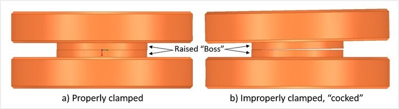
The EIA standard calls for a “raised boss” near the center of the flange. The idea is to ensure that flanges are tightly compressed at the surfaces surrounding the waveguides. The standard achieves the desired purpose when the screws are properly tightened. But in practice, it is easy to improperly tighten the flange screws. This has led to the rise of anti-cocking designs which make it nearly impossible to tilt the waveguides when tightening the screws. Some vendors add intricate cutouts near the waveguides that are designed to 1) promote a tight compression of two mating flanges near the waveguide opening, and 2) suppress RF leakage along the surface between the two flanges. But if the flange faces are sufficiently flat, a good anti-cocking connection can be achieved without the intricate cutouts.
Rectangular Waveguide Loss
You may have seen a graph like the one below which shows rectangular waveguide loss per unit length for various waveguide bands. It is interesting to note that the loss is actually higher at the lower frequencies within a given band. The chart shown is specifically for gold plated waveguides. It is assumed that all of the RF current is contained within the gold layer. Similar charts are available for copper and other metals. These charts provide good estimates of waveguide loss, but there are many variables that can impact accuracy including variations in surface roughness.
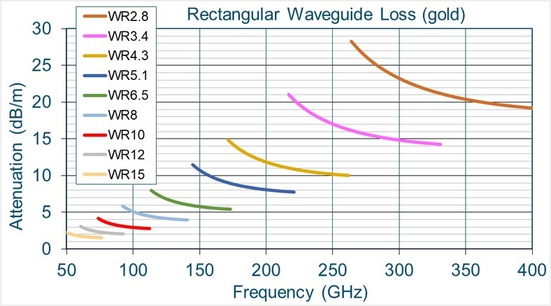
So how good is a rectangular waveguide in terms of loss? A 10 cm long coaxial cable can easily have a loss exceeding 3 dB at 100 GHz (50% of the signal power is lost). In contrast, a 100 GHz signal traversing a 10 cm length of WR-10 waveguide incurs a loss of only (3 dB/m)(0.1 m) = 0.3 dB. Only 7% of the signal power is lost to waveguide conductor loss. Rectangular waveguide losses steadily increase in the higher mm-wave bands. Consider a 300 GHz signal traversing a 10 cm long WR-2.8 waveguide. According to the chart, the loss is (23 dB/m)(0.1 m) = 2.3 dB. In this case, 41% of the signal power is lost. But if you used a WR-3.4 waveguide instead, the loss drops to 1.5 dB (29%). Of course, you won’t see many long runs of WR-2.8 or WR-3.4 waveguide!
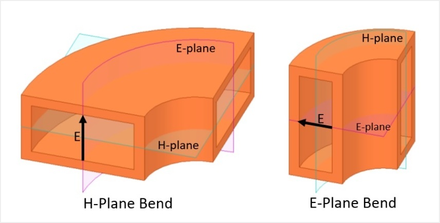
E-plane and H-plane Bends
Don’t you hate it when someone asks you if you want an E-plane bend or an H-plane bend? It can be hard to remember which is which. Perhaps the graphic below is helpful. Here is another helpful reminder. When bending an extruded waveguide, E-plane is the Easy bend to make, and H-plane is the Hard one.
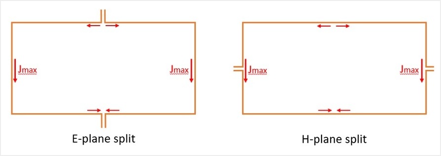
E-plane and H-plane Splits
Split waveguide blocks are easily machined using CNC milling machines. But did you know that the E-plane split is much preferable to the H-plane split? The graphic below shows the E-plane split on the left and the H-plane split on the right. For illustration purposes, large gaps are shown at the split planes. The E-plane split is much preferred since the surface currents in the TE10 mode do not cross the split plane. However, this is not the case with H-plane splits. In fact, the surface current in the primary TE10 mode is at a maximum at the H-plane split. When using an H-plane split, it is necessary to ensure a good electrical connection at all points along the split where they intersect the waveguide edges. Even small gaps and imperfections can cause significant reflections. Extra clamping screws can be used to exert pressure along the joint lines and tighter machining specifications may also be warranted. So why would anyone ever use an H-plane split? Well, sometimes the geometry of the device requires it. Some good examples are Y-junction circulators and orthomode transducers.
Conclusion
Hope you found something of interest in this article. I tried to briefly cover a lot of topics related to rectangular waveguides that are not always covered in textbooks. For more in-depth treatments of rectangular waveguides, I would recommend Microwave Engineering by David Pozar and Advanced Engineering Electromagnetics by Constantine Balanis. If you have any questions regarding this article, feel free to contact Micro Harmonics.